 | –≠–ª–µ–∫—Ç—Ä–æ–Ω–Ω—ã–π –∫–æ–º–ø–æ–Ω–µ–Ω—Ç: LM211N | –°–∫–∞—á–∞—Ç—å:  PDF PDF  ZIP ZIP |

Philips Semiconductors Linear Products
Product specification
LM111/211/311/
LM311B
Voltage comparator
273
August 31, 1994
853-0927 13721
DESCRIPTION
The LM111 series are voltage comparators that have input currents
approximately a hundred times lower than devices like the
µ
A710.
They are designed to operate over a wider range of supply voltages;
from standard
±
15V op amp supplies down to a single 3V supply.
Their output is compatible with RTL, DTL, and TTL as well as MOS
circuits. Further, they can drive lamps or relays, switching voltages
up to 50V at currents as high as 50mA.
Both the inputs and the outputs of the LM111 series can be isolated
from system ground, and the output can drive loads referred to
ground, the positive supply, or the negative supply. Offset balancing
and strobe capability are provided and outputs can be wire-ORed.
Although slower than the
µ
A710 (200ns response time vs 40ns), the
devices are also much less prone to spurious oscillations. The LM111
series has the same pin configuration as the
µ
A710 series.
FEATURES
∑
Operates from single 3V supply (LM311B)
∑
Maximum input bias current: 150nA (LM311--250nA)
∑
Maximum offset current: 20nA (LM311--50nA)
∑
Differential input voltage range:
±
30V
∑
Power consumption: 135mW at
±
15V
∑
High sensitivity--200V/mV
∑
Zero crossing detector
PIN CONFIGURATION
1
2
3
4
5
6
7
8
D, FE, N PACKAGES
GND
INPUT
INPUT
V≠
V+
OUTPUT
BAL/STROBE
BALANCE
+
≠
APPLICATIONS
∑
Precision squarer
∑
Positive/negative peak detector
∑
Low voltage adjustable reference supply
∑
Switching power amplifier
ORDERING INFORMATION
DESCRIPTION
TEMPERATURE RANGE
ORDER CODE
DWG #
8-Pin Plastic Dual In-Line Package (DIP)
-55
∞
C to +125
∞
C
LM111N
0404B
8-Pin Plastic Dual In-Line Package (DIP)
-25
∞
C to +85
∞
C
LM211N
0404B
8-Pin Plastic Small Outline Package (SO)
0 to +70
∞
C
LM311D
0174C
8-Pin Plastic Dual In-Line Package (DIP)
0 to +70
∞
C
LM311N
0404B
8-Pin Plastic Small Outline Package (SO)
-25
∞
C to +85
∞
C
LM211D
0174C
8-Pin Ceramic Dual In-Line Package (CERDIP)
-55
∞
C to +125
∞
C
LM111FE
0580A
8-Pin Plastic Small Outline Package (SO)
0 to +70
∞
C
LM311BD
0174C
8-Pin Plastic Dual In-Line Package (DIP)
0 to +70
∞
C
LM311BN
0404B
Philips Semiconductors Linear Products
Product specification
LM111/211/311/
LM311B
Voltage comparator
August 31, 1994
274
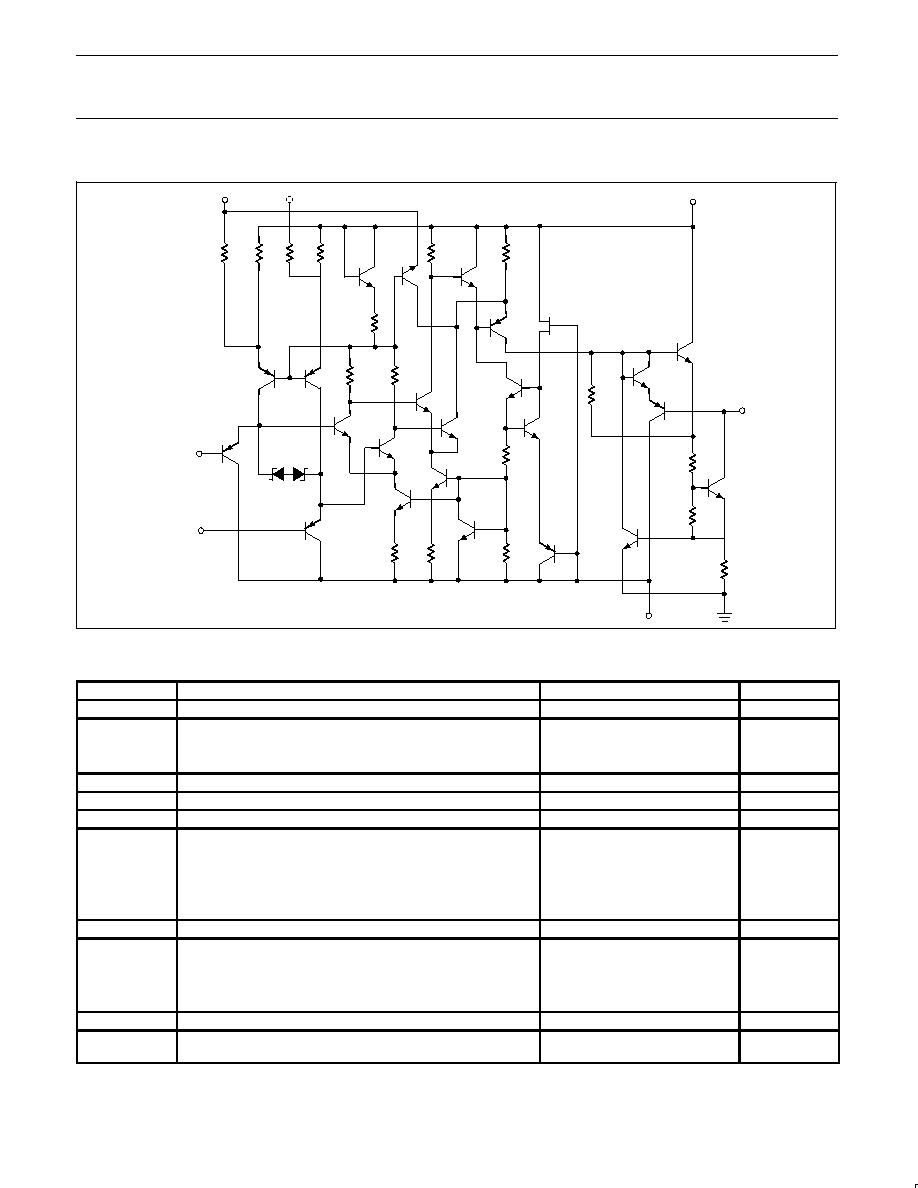
EQUIVALENT SCHEMATIC
BALANCE/
STROBE
BALANCE
R3
300
R1
1.3K
R4
300
R2
1.3K
Q8
R5
70
Q5
R6
1.2K
R7
1.2K
Q7
Q3
R8
750
Q10
R9
600
Q11
Q20
Q19
Q8
Q9
Q18
R10
4K
Q13
Q12
Q14
OUTPUT
V+
Q15
R11
130
R12
600
R13
4
Q18
V≠
Q17
R15
450
R15
400
R14
2K
R17
60
Q22
R18
200
Q4
Q2
Q23
R19
250
Q2
D1
5V
D2
5V
Q1
INPUTS
ABSOLUTE MAXIMUM RATINGS
SYMBOL
PARAMETER
RATING
UNIT
V
S
Total supply voltage
36
V
Output to negative supply voltage:
LM111/LM211
50
V
LM311/LM311B
40
V
Ground to negative supply voltage
30
V
Differential input voltage
±
30
V
V
IN
Input voltage
1
±
15
V
P
D MAX
Maximum power dissipation,
T
A
=25
∞
C (still-air)
2
F package
810
mW
N package
1190
mW
D package
780
mW
I
Output short-circuit duration
10
sec
T
A
Operating ambient temperature range
LM111
-55 to +125
∞
C
LM211
-25 to +85
∞
C
LM311/LM311B
0 to +70
∞
C
T
STG
Storage temperature range
-65 to +150
∞
C
T
SOLD
Lead soldering temperature
(10sec max)
300
∞
C
NOTES:
1. This rating applies for
±
15V supplies. The positive input voltage limit is 30V above the negative supply. The negative input voltage limit is
equal to the negative supply voltage or 30V below the positive supply, whichever is less.
2. Derate above 25
∞
C, at the following rates: F package at 6.4mW/
∞
C; N package at 9.5mW/
∞
C; D package at 6.2m/W
∞
C
Philips Semiconductors Linear Products
Product specification
LM111/211/311/
LM311B
Voltage comparator
August 31, 1994
275
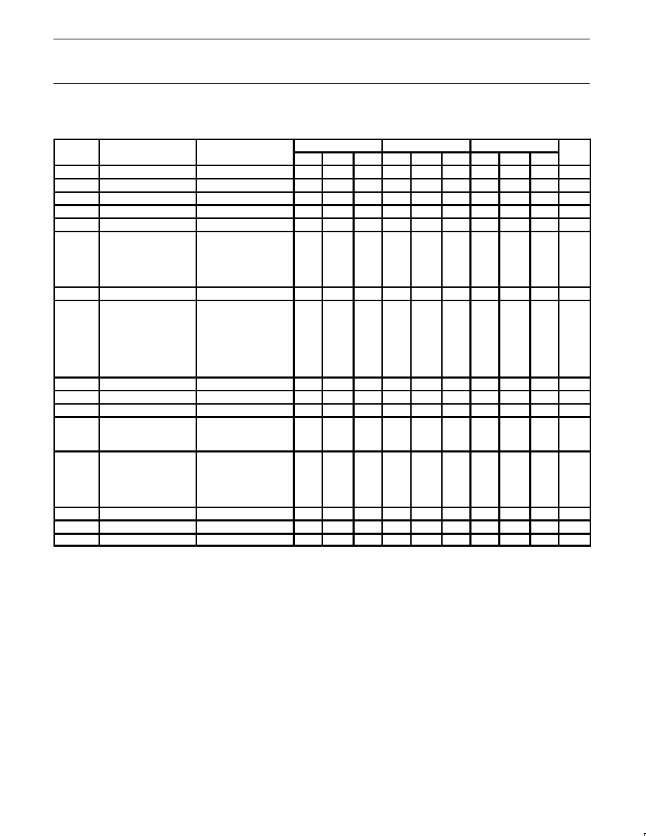
DC ELECTRICAL CHARACTERISTICS
1, 2, 3, 6
Over temperature range unless otherwise specified.
SYMBOL
PARAMETER
TEST CONDITIONS
LM111/LM211
LM311
LM311B
UNIT
SYMBOL
PARAMETER
TEST CONDITIONS
Min
Typ
Max
Min
Typ
Max
Min
Typ
Max
UNIT
V
OS
Input offset voltage
3
T
A
=25
∞
C, R
S
50k
0.7
3.0
2.0
7.5
2.0
7.5
mV
I
OS
Input offset current
3
T
A
=25
∞
C
4.0
10
6.0
50
6
25
nA
I
BIAS
Input bias current
T
A
=25
∞
C
60
100
100
250
100
200
nA
A
V
Voltage gain
T
A
=25
∞
C
200
200
200
V/mV
Response time
4
T
A
=25
∞
C
200
200
500
ns
V
SAT
Saturation voltage
LM111/211 V
IN
-5mV,
I
OUT
=50mA
LM311/B V
IN
-10mV,
I
OUT
=50mA
T
A
=25
∞
C
0.75
1.5
0.75
1.5
0.75
1.5
V
I
BAL/STR
Strobe on current
T
A
=25
∞
C
3.0
3.0
3.0
mA
I
LEAKAGE
Output leakage current
6
LM111/211 V
IN
5mV,
V
OUT
=35V
LM311/B V
IN
10mV,
V
OUT
=35V
T
A
=25
∞
C,
I
STROBE
=3mA
(V≠ = V
GND
= ≠5V)
0.2
10
0.2
50
0.2
50
nA
V
OS
Input offset voltage
3
R
S
50k
4.0
10
10
mV
I
OS
Input offset current
3
20
70
50
nA
I
BIAS
Input bias current
150
300
250
nA
V
IN
Input voltage range
V=
±
15V (Pin 7 may go
to 5V)
-14.5
13.8
to
-14.7
13.0
-14.5
13.8
to
-14.7
13.0
V≠
+0.5
V+
≠1.5
V
V
OL
Saturation voltage
6
V+
4.5V, V- = 0
LM111/211 V
IN
-6mV,
I
SINK
8mA
LM311/B V
IN
-10mV,
I
SINK
8mA
0.23
0.4
0.23
0.4
0.23
0.4
V
I
OH
Output leakage current
V
IN
5mV, V
OUT
=35V
0.1
0.5
µ
A
I
CC
Positive supply current
T
A
=25
∞
C
5.1
6.0
5.1
7.5
1.6
3.5
mA
I
EE
Negative supply voltage
T
A
=25
∞
C
4.1
5.0
4.1
5.0
mA
NOTES:
1. This rating applies for
±
15V supplies. The positive input voltage limit is 30V above the negative supply. The negative input voltage limit is
equal to the negative supply voltage or 30V below the positive supply, whichever is less.
2. These specifications apply for V
S
=
±
15V and 0
∞
C < T
A
< 70
∞
C unless otherwise specified. With the LM211, however, all temperature
specifications are limited to -25
∞
C
T
A
85
∞
C and for the LM111 is limited to -55
∞
C T
A
< 125
∞
C. The offset voltage, offset current, and bias
current specifications apply for any supply voltage from a single 5V supply up to
±
15V supplies.
3. The offset voltages and offset currents given are the maximum values required to drive the output within a volt of either supply with 1mA
load. Thus, these parameters define an error band and take into account the worst case effects of voltage gain and input impedance.
4. The response time specified is for a 100mV input step with 5mV over-drive.
5. Do not short the strobe pin to ground; it should be current driven at 3mA to 5mA.
6. LM311B, all parameters are at V+ = 3V
±
10%, V≠ = GND = 0V.
Philips Semiconductors Linear Products
Product specification
LM111/211/311/
LM311B
Voltage comparator
August 31, 1994
276
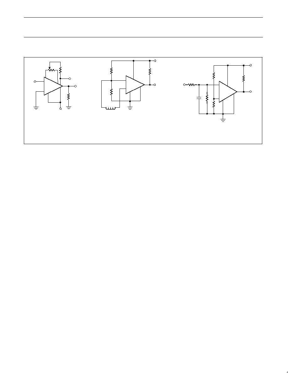
TYPICAL APPLICATIONS
INPUT
R1
3K
BAL
R2
3K
V+ = 5V
TO
MOS
LOGIC
R3
10K
V≠ = 10V
5
6
8
7
1
4
3
2
INPUT
+
≠
LM311
+
≠
LM311
V+ 5V
R3
2K
TTL
OUTPUT
8
7
3
2
4
1
R1
4.5K
R2
1K
MAGNETIC
PICKUP
+
≠
LM311
V+ = 5V
TO TTL
OUTPUT
2
3
8
7
1
4
R4
82K
R2
47K
C1
R1
240K
R3
82K
R5
1K
Zero Detector
Driving MOS Logic
Detector for Magnetic
Transducer
TTL Interface with High
Level Logic
* Values shown are for a 0 to 30V logic swing and a 15V threshold.
** May be added to control speed and reduce susceptibility to noise spikes.